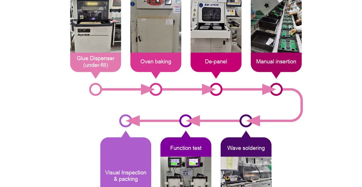
Inspection and testing equipment play a critical role in the Surface Mount Technology (SMT) process by ensuring high-quality PCB assembly, minimizing defects, and improving production efficiency. These systems detect placement errors, soldering defects, and electrical failures, helping manufacturers maintain high reliability and yield rates. Below is how different inspection and testing equipment fit into the SMT assembly process.
1. Solder Paste Inspection (SPI) – Before Component Placement
Purpose:
- Ensures that solder paste is correctly applied to PCB pads before components are placed.
- Detects insufficient paste, excessive paste, bridging, and misalignment.
How It Works:
- Uses 3D laser scanning and imaging to measure solder paste volume, height, and coverage.
- Compares actual deposits with CAD data to identify deviations.
Why It’s Important:
- Prevents soldering defects before they occur, reducing rework.
- Ensures uniform paste distribution, improving solder joint reliability.
2. Automated Optical Inspection (AOI) – After Pick-and-Place & After Reflow Soldering
Purpose:
- Detects component misalignment, missing parts, incorrect polarity, and soldering defects.
How It Works:
- Uses high-resolution cameras, 3D imaging, and pattern recognition AI to analyze PCB assembly quality.
- Identifies incorrectly placed components, open circuits, and insufficient soldering.
Why It’s Important:
- Reduces defective boards before final testing, improving yield rates.
- Speeds up quality control by replacing slow manual inspection.
- Detects defects before final soldering becomes permanent, saving rework costs.
3. X-ray Inspection (AXI) – For Hidden Solder Joints (BGAs, QFNs, and Multi-Layer PCBs)
Purpose:
- Detects hidden solder defects in Ball Grid Arrays (BGAs), Quad Flat No-Leads (QFNs), and multilayer PCBs.
- Identifies issues like voids, solder bridges, and incomplete connections under components.
How It Works:
- Uses X-ray imaging to see through PCBs and analyze solder joints beneath components.
- AI-powered software compares solder patterns to detect defects.
Why It’s Important:
- Essential for high-density PCB designs where solder joints are not visible to AOI.
- Prevents hidden electrical failures in automotive, aerospace, and medical electronics.
- Ensures BGA and QFN components are properly soldered, reducing field failures.
4. Functional Circuit Testing (FCT) – After PCB Assembly
Purpose:
- Verifies that the assembled PCB operates correctly under real-world conditions.
How It Works:
- Powers up the board and tests voltage levels, signal integrity, and component functionality.
- Simulates actual operating conditions using test jigs, fixtures, and software diagnostics.
Why It’s Important:
- Identifies electrical malfunctions early, reducing post-assembly troubleshooting.
- Ensures all components are working before final product assembly.
- Prevents defective products from reaching end-users, improving brand reputation.
5. In-Circuit Testing (ICT) – Electrical Component Verification
Purpose:
- Checks for open circuits, short circuits, component values, and solder joint integrity.
- Ensures resistors, capacitors, and ICs are correctly placed and functioning.
How It Works:
- Uses a bed-of-nails test fixture to probe PCB test points.
- Measures voltage, resistance, and current to verify circuit behavior.
Why It’s Important:
- Identifies defective components early, preventing costly rework.
- Detects soldering defects and missing connections.
- Provides fast and accurate pass/fail results for high-volume production.
6. Flying Probe Testing – Alternative to ICT for Low-Volume Production
Purpose:
- Used when ICT fixtures are too expensive for low-volume or prototype testing.
- Detects short circuits, open circuits, and incorrect component values.
How It Works:
- Uses moving robotic probes to contact test points without needing a fixed fixture.
- Verifies electrical integrity and basic circuit operation.
Why It’s Important:
- Ideal for prototype and low-volume production, eliminating the cost of ICT test fixtures.
- Provides flexibility by testing different PCB designs without reconfiguration.
- Helps identify early-stage design errors before mass production.
7. Environmental and Burn-In Testing – Ensuring Long-Term Reliability
Purpose:
- Simulates extreme temperature, humidity, and mechanical stress to verify PCB durability.
- Identifies weaknesses in solder joints, PCB materials, and component integrity.
How It Works:
- Thermal cycling chambers expose PCBs to rapid temperature shifts.
- Vibration and shock testing check mechanical durability.
- Humidity and corrosion testing simulate harsh environments.
Why It’s Important:
- Essential for automotive, aerospace, and military electronics.
- Ensures PCBs can withstand real-world conditions without premature failure.
- Helps manufacturers comply with industry safety standards.
How These Inspection and Testing Steps Fit Into the SMT Process
- Solder Paste Inspection (SPI) → Ensures correct solder paste application before component placement.
- Automated Optical Inspection (AOI) → Detects placement errors before and after reflow soldering.
- X-ray Inspection (AXI) → Verifies hidden solder joints for BGAs and QFNs.
- In-Circuit Testing (ICT) / Flying Probe Testing → Checks component placement and solder joint quality.
- Functional Circuit Testing (FCT) → Ensures the PCB operates correctly under real-world conditions.
- Environmental and Burn-In Testing → Confirms long-term reliability in harsh environments.
Conclusion
Inspection and testing equipment are essential for detecting and preventing defects in the SMT process. From solder paste inspection and AOI to X-ray, ICT, and functional testing, these systems ensure high-quality, defect-free PCB assembly. By integrating automated inspection and real-time testing, manufacturers can reduce rework, improve yield rates, and ensure reliable electronics in mass production.
Hashtags
#SMTInspection #TestingEquipment #QualityControl #SurfaceMountTechnology #PCBAssurance #PCBTesting #AOITesting #AutomatedInspection #OpticalInspection #SMTQuality #DefectDetection #AXI #XRayInspection #HiddenSolderJoints #BGAInspection #NonDestructiveTesting #SolderPasteInspection #SPI #StencilPrinting #SMTPrinting #PCBPrecision #ICTTesting #InCircuitTesting #PCBFunctionality #ElectricalTesting #FCT #FunctionalTesting #EndProductReliability #PerformanceTesting #ElectronicsTesting #AIinInspection #AutomatedQualityControl #MachineLearning #Industry40 #PredictiveMaintenance #SmartTesting


