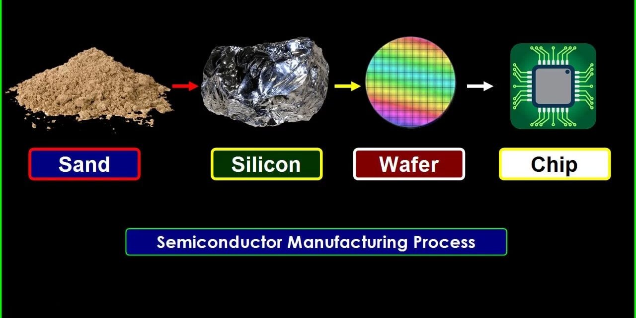
The semiconductor manufacturing process is a highly complex and precise procedure that transforms raw materials into functional microchips used in a wide range of electronic devices, such as smartphones, computers, cars, and medical equipment. The process involves several stages, from designing the semiconductor to the final production of integrated circuits (ICs) or microchips. Here’s an overview of the semiconductor manufacturing process:
1. Design Phase
- Circuit Design: Before any physical work begins, engineers design the semiconductor device at the circuit level. This step involves creating a schematic of the integrated circuit (IC), which specifies how individual components (transistors, capacitors, etc.) will be connected.
- Layout Design: After the circuit design, the next step is to design the layout, which defines the physical arrangement of the circuit elements on the semiconductor wafer. This layout is translated into a pattern that will later be etched onto the wafer.
- Simulation: The design undergoes simulation to ensure the circuit functions as intended and meets performance requirements like speed, power consumption, and heat dissipation.
2. Wafer Production
- Material Selection: The process starts with a silicon wafer, as silicon is the most commonly used semiconductor material. Silicon wafers are made from silicon crystals grown using a method called the Czochralski process, where a silicon crystal is pulled from molten silicon.
- Wafer Preparation: The silicon crystal is sliced into thin, circular wafers, usually around 200-300 millimeters in diameter. These wafers are then polished to create a smooth, flat surface suitable for processing.
3. Photolithography
- Coating with Photoresist: A thin layer of photoresist material is applied to the surface of the silicon wafer. Photoresist is a light-sensitive substance that will react to light in specific patterns.
- Masking: A photomask, which contains the pattern of the circuit design, is placed over the wafer. The wafer is then exposed to ultraviolet (UV) light, which passes through the mask and exposes the photoresist on the wafer. The areas that are exposed to the UV light will undergo a chemical change.
- Development: After exposure, the wafer is treated with a developer solution that removes either the exposed or unexposed photoresist, depending on whether the photoresist is positive or negative. This process leaves behind a pattern of photoresist that matches the desired circuit layout.
4. Etching
- Etching the Wafer: The wafer is then exposed to etching chemicals (e.g., acids or gases) to remove the unprotected parts of the wafer surface, leaving behind the desired pattern of circuit elements.
- Types of Etching: Etching can be done in two ways:
- Wet Etching: Uses liquid chemicals to dissolve the material.
- Dry Etching: Uses gases and plasma (ionized gases) to etch the material, allowing for more precise control and finer features.
- This process creates the microscopic structures of transistors, wires, and other components on the wafer.
5. Doping (Ion Implantation)
- Doping is the process of introducing impurities (dopants) into the silicon wafer to modify its electrical properties and create P-type and N-type regions.
- Ion Implantation: In this process, dopants are accelerated and implanted into the wafer in a controlled manner. The dopants are selectively introduced into specific regions of the wafer, creating the PN junctions needed for transistors and diodes.
- The doping process determines the electrical characteristics of the semiconductor, such as its ability to conduct or insulate electricity.
6. Deposition
- Thin Film Deposition: A thin layer of material (often metal or silicon dioxide) is deposited on the wafer’s surface. This layer can serve as an insulating material or a conductive layer for wiring.
- Chemical Vapor Deposition (CVD): A common technique for depositing thin films where gases react at high temperatures to form solid material, which then condenses on the wafer surface.
- Physical Vapor Deposition (PVD): Another method that involves heating material in a vacuum chamber to create vapor, which condenses onto the wafer.
7. Chemical-Mechanical Planarization (CMP)
- After multiple deposition and etching steps, the wafer surface can become uneven or rough. CMP is used to smooth and flatten the surface of the wafer.
- This is achieved by using a combination of chemical slurry and mechanical polishing to remove excess material, ensuring the wafer is uniformly flat before proceeding with further steps.
8. Metallization
- Metal Layers: After the transistor structures are formed, metal layers (usually copper or aluminum) are deposited on the wafer and etched to form the wiring that connects different components of the circuit.
- This allows the transistors to communicate with each other and form a complete functional circuit.
9. Packaging
- Wafer Cutting: Once the wafer has been processed and the circuit structures are formed, the wafer is cut into individual chips or dies using a technique called dicing. Each die is a complete, functional microchip.
- Die Bonding: The individual chips are then attached to a package, which will house the chip and provide connections to the external world.
- Wire Bonding: Fine gold or aluminum wires are used to connect the chip’s bonding pads to the leads of the package, which allows for electrical connections between the chip and the outside world.
- Encapsulation: The chip is encapsulated with a protective material to shield it from physical damage, moisture, and contaminants.
10. Testing and Quality Control
- Electrical Testing: The final chips are tested to ensure they meet the required specifications. This can include tests for speed, power consumption, and reliability under different conditions (e.g., voltage, temperature).
- Final Inspection: Each chip is inspected for physical defects using automated optical inspection systems. Chips that pass all the tests are packaged and ready for use, while defective ones are discarded or reworked.
11. Final Packaging and Shipment
- After passing the testing phase, the chips are packaged into their final form, ready for shipment to manufacturers for integration into consumer electronics or other applications.
- Some semiconductors are sold in bulk, while others are integrated into modules or systems before being shipped out.
Conclusion
The semiconductor manufacturing process is a highly intricate and multi-step procedure that transforms basic materials like silicon into the microchips that power virtually all modern electronics. Advanced technologies, like photolithography at nanometer scales, ion implantation, and chemical vapor deposition, allow manufacturers to create chips with ever-decreasing sizes and increasing performance. The industry continues to advance, with constant innovation in manufacturing techniques to meet the growing demand for more powerful, efficient, and compact electronic devices.
Hashtags
#WaferFabrication #SemiconductorWafers #WaferProcessing #WaferManufacturing #SemiconductorWafer #SiliconWaferTech #WaferCleanroom #Photolithography #LithographyProcess #SemiconductorMasking #Photomasks #PhotolithographyTech #ChipPatterning #MicrochipLithography #Doping (Ion Implantation) #DopingSemiconductors #IonImplantation #SemiconductorDoping #IonBeamDoping #SemiconductorIonImplantation


